Semi Wafer

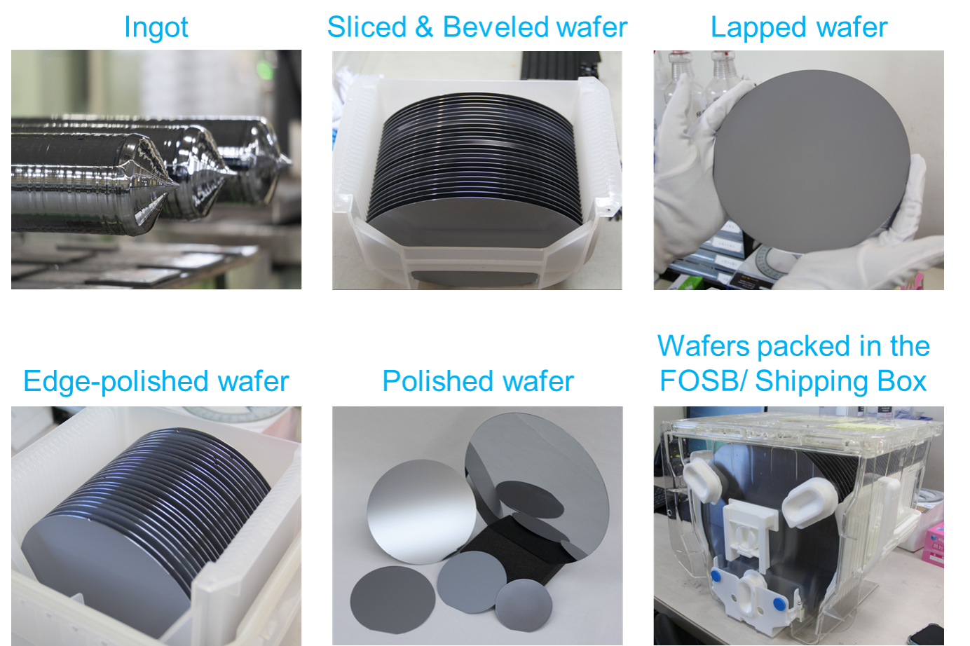
ACC has demonstrated decades of outstanding skills and techniques on ingot growth and diamond wire wafer slicing, going with state-of-the-art wafer beveling and lapping process to deliver high quality and customized products to our valued customers.


8”Semi Wafer Specification


Item

Specification

Conductivity

P / N

Dopant Type

Boron / Phosphorus

Outer Diameter (mm)

200 ±.0.2

Resistivity (Ω cm)

≧0.5 (standard specification)

< 0.05 (high dope specification)

Thickness (μm)

725 ±25 (standard specification)

550~1,000 (customized specification)

LPD

≦50ea(≧0.12μm)or ≦20ea(≧0.2μm)

SurfaceMetal Impurity (atoms/cm2)

≦1E+10

12”Semi Wafer Specification


Item

Specification

Conductivity

P / N

Dopant Type

Boron / Phosphorus

Outer Diameter (mm)

300 ±.0.2

Resistivity (Ω cm)

≧0.5 (standard specification)

< 0.05 (high dope specification)

Thickness (μm)

775 ±25 (standard specification)

LPD

65nm<50ea, 40nm<100ea

SurfaceMetal Impurity (atoms/cm2)

≦1E+10